PCB Layout
-
60,000 pins Communication Board Design Case

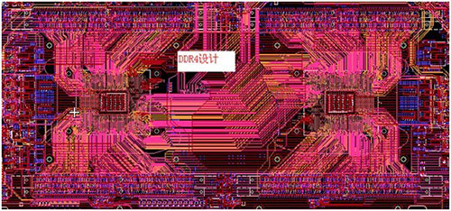
【Product】: 60,000 pins Communication Board Design Case 【Background】: There are more than 60,000 pins on this board and the space for placement is extremely limited. Also, the lead time is quite short. It was required to finish the design, SI simulation and fabrication within two months. What’s more, EDADOC started to design this PCB even when the schematic diagram has not been confirmed. We were doing the layout and simulation work while the schematic was still being reviewed. There are lots of power supplies of low voltage and high current, and many different types of interfaces on the board which required high speed. 【Interface Type】: SFP+, Interlaken, QPI, PCIE3, DDR4 , DDR3, etc. 【Standard】: SFF8431,QPI3.0,PCIE3.0,JESD79-4,JESD79-3E, etc. 【Speed Rates】: 1.PCIE3.0 -8Gbps;
2.PCIE2.0- 5Gbps;
3.QPI- 9.6Gbps;
4.DDR4- 2133Mbps;
5.DMI- 5Gbps;
6.Interlaken- 12.5Gbps/10.3125Gbps;
7.DDR3- 1600Mbps;
8. serdes-10.3125Gbps. -
Notebook mainboard

【Type】: NotebookTypical notebook mainboard 【Difficulty】: Ⅰ.This product adopts an Intel Centrino chip;
Ⅱ.The North Bridge and the CPU are not in the same side;
Ⅲ.Features: cross connection of 800MHz FSB bus, 6-layer board, and small routing layers.
Ⅳ.It is required to have less routing on the surface layer as this board will be provided to the third party as a reference board and the board should be designed strictly according to the "Yellow Book"
Ⅴ.The coverage rate of ICT should reach 95% (including the single-point network)【Countermeasure】: Ⅰ.Thorough research on the characteristics of pin definitions, comprehensive planning;
Ⅱ.Properly would lines inside the North Bridge and the CPU;
Ⅲ.Fully understanding of the key degree of signals, treated them respectively, and distributed important signals in priority routing layers:
Ⅳ.Upon placement, we considered ICT requirements, and left necessary space for ICT. Multi-person concurrent design assured the board design progress;【Result】: The first version of the demo board was debugged successfully, so it was very smooth to conduct software debugging.
-
Name A Second-Order HDI Cell Phone Board

【TYPE】: Typical high-end consumer electronic product board 【Difficulty】: Ⅰ.Very small, its main board is half the size of a common cell phone board.
Ⅱ.Strange shape results in great limits for routing;
Ⅲ.GSM & WCDMA dual-mode cell phone results in a large radio-frequency area.
Ⅳ.Super-thin cell phone solution limits the board thickness; placing the whole radio-frequency module under the baseband chip results in great limits in hole drilling on the baseband chip;
Ⅴ.Originally, ALIVH materials was to be used, but considering cost and risk reduction, we used second-order buried via scheme, but the routing requirements were not degrade.【Countermeasure】: Ⅰ.By discussing with multiple PCB manufacture partners, we set appropriate design parameters;
Ⅱ.With RF experts' participation in PCB design, strict design process assured signal quality of the board;
Ⅲ.Careful optimization achieved the best coordination among requirements of different parties;【Result】: Design fulfilled according to the plan, successful CAM and smooth debugging. -
Name Switching Board of L3 Core Routing Switch

【TYPE】: Typical high-speed board 【Difficulty】: Ⅰ.Using BCM56601 chipset scheme with RLDRAM, DDRII SDEAM, TCAM;
Ⅱ.Strict requirement for time sequence;
Ⅲ.Multiple pairs of 3.12G signals, 48 pairs of 1.25G signals, and each pair of signal is 13 inches long;
Ⅳ.Strictly controlled impedance, various kinds of power supplies, 8 kinds of current above 6 Amperes, a large number of phase lock loops (PLLs);
Ⅴ.The number of pins on a board is more than 25000, and a large number of network rules;【Countermeasure】: Ⅰ.Making detailed data analysis to calculate time sequence, HSPICE simulates the routing rules of 1.25G signals and 3.125G signals;
Ⅱ.Pre-simulation determines the routing topology of RLDRAM, DDEIISDEAM and TCAM, and post-simulation assures their time sequence;
Ⅲ.Reasonably design current routing channels through current calculating software;
Ⅳ.Multi-person concurrent design ensures board design process;【Result】: Completion time of board design is half of the customer's estimated time, and the signal quality complies with the requirements. -
Name PMC (Pic Mezzanine Card)

【TYPE】: Typical high-speed &high-density HDI board 【Difficulty】: Ⅰ.18 pieces of DDRII chips mounted on both face and back;
Ⅱ.High-density placement, strict topology structure and time sequence relation;
Ⅲ.Multiple large currents, and strict heat design to meet clients' requirements;【Countermeasure】: Ⅰ.Making detailed data analysis to calculate time sequence;
Ⅱ.Conducting pre-simulation to determine DDRII' s routing topology, and delete some unnecessary matching resistance.
Ⅲ.Conducting post-simulation to assure their time sequence;
Ⅳ.Reasonable design current routing channels through current calculating software;
Ⅴ.Using HDI design to meet density requirements;
Ⅵ .Multi-person concurrent design ensures board design progress;【Result】: Completion time of board design is half of the customer's estimated time, and the signal quality complies with the requirements. -
High-speed backplane for optical network product

【TYPE】: High-speed backplane for optical network product 【Difficulty】: More than 320 differential pairs with 3.125G signal. And 640+ differential pairs with 3.125G signal. The PCB size is 653 X 418. The Insertion loss is a big problem with long trace. And return loss is also a problem in case the impedance mismatch. We also considering the crosstalk and EMI. 【Solution】: Extract Via model and trace model in HFSS. Eye diagram Simulation with HSPICE.S parameter analysis for Insertion loss and return loss. 【Result】: Reduce the layer from 32 to 28 with good signal quality. It's better for PCB fabrication. -
Single board with more than 69000Pins

【TYPE】: Single board with more than 69000Pins 【Difficulty】: Design is quite complicated. There are six ICs with more than 2600 pins and 48 piece of DDR3 chips. The board is 26 layers with many High speed signals. The PCB file is more than 356M. 【Solution】: A whole design team include SI engineer is involved into this project. By using design partition tools and onsite communication, we finish this design in 2 months. Then spend nearly one month for review and optimize. 【Result】: Project is very successful by good team work and professional Skills. -
10G High speed backplane in 28 layers

【TYPE】: 10G High speed backplane in 28 layers 【Difficulty】: Thousands of 10G high-speed differential pairs in this backplane. Signal integrity is very important for this design. 【Solution】: With the experienced in PCB design and manufacture for many years. EDADOC co-work with the PCB suppliers and connector suppliers, and communication with customers closely. SI team is involved into this project. The SI process is Pre-simulation, Constraint driven PCB design, and Post simulation for verification. 【Result】: The first version of this project was debugged successfully. The quality of signal is fulfill with the Spec. -
TYPEⅢ HDI PCB Design for OMAP4430 Platform

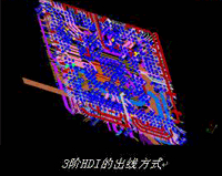
【TYPE】: TYPEⅢ HDI PCB Design for OMAP4430 Platform 【Difficulty】: There are two 0.4 mm pitch IC in this design with extreme density. So we have to choose TYPEⅢ HDI PCB design. This project is a reference designs board of Intel. The quality and schedule are both very important. 【Solution】: In this project, with the experienced in PCB design and manufacture, EDADOC provide many Suggestions to help customers reduce the restrictions in batch production process. At the same time, EDADOC realize the 24 hours continuous work teamwork between North America and China site. Ensure the schedule of this project. 【Result】: Finally this project is successful in first prototype. Reduce the time to market and earn the good opportunities. This design become benchmarking of EDADCO for TYPEⅢ HDI PCB Design.


