60,000 pins Communication Board Design Case
<<BackSource:Edadoc Time:2014/10/25 0:00:00
http://www.en.edadoc.com/Company/AboutEdadoc
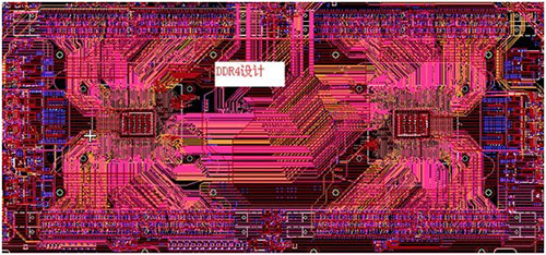
(1)DDR4 routing
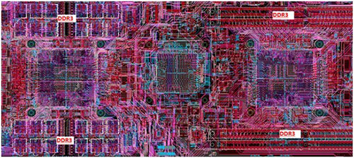
(2)DDR3 routing
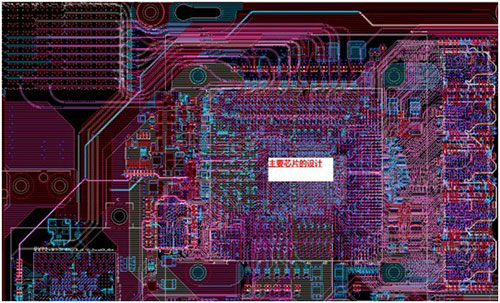
(3)Main Chips routing
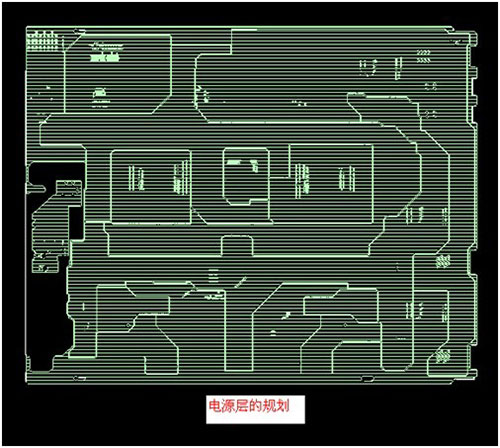
(4)Power Plane
| 【Product】: |
60,000 pins Communication Board Design Case |
| 【Background】: | There are more than 60,000 pins on this board and the space for placement is extremely limited. Also, the lead time is quite short. It was required to finish the design, SI simulation and fabrication within two months. What’s more, EDADOC started to design this PCB even when the schematic diagram has not been confirmed. We were doing the layout and simulation work while the schematic was still being reviewed. There are lots of power supplies of low voltage and high current, and many different types of interfaces on the board which required high speed. |
| 【Interface Type】: | SFP+, Interlaken, QPI, PCIE3, DDR4 , DDR3, etc. |
| 【Standard】: | SFF8431,QPI3.0,PCIE3.0,JESD79-4,JESD79-3E, etc. |
| 【Speed Rates】: |
1.PCIE3.0 -8Gbps; 2.PCIE2.0- 5Gbps; 3.QPI- 9.6Gbps; 4.DDR4- 2133Mbps; 5.DMI- 5Gbps; 6.Interlaken- 12.5Gbps/10.3125Gbps; 7.DDR3- 1600Mbps; 8. serdes-10.3125Gbps. |
| 【Simulation Description】: | In this project, the high-density placement, the various types of power supply and high-speed signals—the highest is 12.5G, required the comprehensive plan for routing layer, and the good signal quality. By simulation, we decided to adopt the low dielectric constant: TU872SLK-sp and the high-speed signal for back drill design; make overall placement for power channel so that the high-current power supply guarantees the enough flow plane. As a result, our design meets the client’s requirement. |
(1)DDR4 routing

(2)DDR3 routing

(3)Main Chips routing

(4)Power Plane

Prev:Nothing
Next:TYPEⅢ HDI PCB Design for OMAP4430 Platform


