The Vice President of EDADOC, Bruce Wu, Interviewed with IConnect007
<<BackSource:Edadoc Time:2017/12/1
The interview focuses on EDADOC’s HDI progress and some of the current trends EDADOC is seeing in HDI. Bruce Wu, the Vice President of EDADOC, interviewed with Andy Shaughnessy,the Managing Editor of IConnect007.
The interview is first published on IConnect007.
See http://iconnect007.uberflip.com/i/899995-pcbd-nov2017/50
Andy Shaughnessy: Tell us a little bit about your company.
Bruce Wu: EDADOC was founded in 2003. We focus primarily on high-speed turn-key PCB services, including PCB design, Fabrication, Assembly and Parts sourcing. We are now the largest high-speed PCB design bureau with more than 500 engineers.
We lanuched our PCB fabrication business in 2009 and currently have factories located in Shenzhen and Sihui, China, capable of providing 2-64 layers of PCB fabrication for both prototype and mass production. We build the first quick turn SMT factory in China. W also offer testing and box building services.
Andy Shaughnessy: What percentage of your designs are HDI?
Bruce Wu: Each year, our company creates over 10,000 single board designs. HDI PCBs make up 10% of this total. The percentage is not very high, because we make designs for a wide range of industries, including communications, medical equipment, computers, industrial control, aerospace, military, consumer electronics and other products. HDI is mainly used in thin and light consumer electronics products, but is not commonly used in communications, medical, aerospace and other fields where reliability is emphasized.
Andy Shaughnessy: Are these primarily for the domestic market in China?
Bruce Wu: At Edadoc, we see demand for HDI technology in the Chinese, North American & Japanese markets where our offices are. HDI technology enables the design of end products to be more miniaturized while meeting the higher standards of electronic performance and efficiency. It is currently widely used in mobile phones as well as digital cameras, notebook computers, automotive electronics and more. There is market demand for HDI in both domestic and overseas markets.
Andy Shaughnessy: What are the biggest challenges you face with your HDI designs?
Bruce Wu: The small board size, more functional modules, and packaging miniaturization (0.35-0.5mm BGA) all cause a design bottleneck. As a result, smaller line widths (<3 mils) and multi-level HDI designs need to be used.
The design of multi-stage HDI requires a flexible and powerful constraint manager that recognizes both micro via and common mechanical holes and sets the spacing constraint between micro via and other elements. The constraints of the network become complicated, and need to support the check-up of the network spacing constraints in various situations. In order to help the design engineers manage projects, we require the ability to clearly display different types of vias.
With Cadence’s powerful miniaturization design tools, combined with their HDI design and processing capabilities, Edadoc has completed countless high-density miniaturization product design tasks.
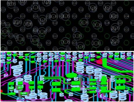
Figure 1 depicts one such design case of a 3-stage HDI board completed by Edadoc’s experienced HDI design team using the Cadence design platform. The density, design of the minimum line width and spacing of 2.4 mils challenged the industry’s limits. Edadoc Technology also helped this customer with the system board fabrication and assembly using its own PCB manufacturing facilities.
Andy Shaughnessy: What trends are you seeing in HDI?
Bruce Wu:
DESIGN:
The emergence of HDI technology is responsible for the growth of the PCB industry. It allows the PCB to be populated with denser BGA and QFP parts. With the development of high-speed serial bus technology, signal transmission rate continues to increase, and the impact of the parasitic parameters has drawn more and more attention. Engineers are studying ways to reduce the effects of parasitics in vias. Due to the design requirements of vias-in-pads, you can reduce the parasitic surface device parameters. Therefore, HDI is also gradually applied to high-speed PCB design, to avoid high-speed signal STUB too long.
PRODUCTION:
HDI board technology development will be presented:
Line refinement: line width / line spacing will transition from the current mainstream (3/3) to the future (2/2).
Multi-order HDI: the order of HDI from the current mainstream (2 + n +2) order transition to the future (any order HDI / class carrier boards)
TERMINAL APPLICATION:
Mobile phones are the traditional market of HDI boards. At present, nearly all of this generation’s intelligent machines use HDI as the motherboard and the expansion rate has been improving at a slow rate. However, HDI may be replaced by higher process level carrier boards in some of the next generation’s models. Now that the market is being saturated with smart phones, the market growth will continue to slow down.
In addition to the advantages of high wiring density and high signal integration, HDI also has better electrical performance and signal integrity in data communications, so future opportunities will be emerging in automotive electronics and communications base stations. In the automotive electronics industry, navigation modules, Bluetooth communication modules and data modules require the use of HDI boards. Car electronics, communications base stations, medical equipment and other emerging product areas continue to rise in absolute terms of incremental growth rate, far beyond the traditional 3C products. It is projected to overtake the smart phone market as the main growth point for HDI technology.
Andy Shaughnessy: What is the "Cutting Edge" for HDI, in space and trace sizes?
Bruce Wu: With the narrowing of HDI line width and line spacing, it is a tremendous challenge to maintain task levels and equipment processing capabilities, especially during exposure, photo development and etching. The thickness to radius ratio of laser drilling machines has increased from 0.75: 1, to 1: 1. And the appearance of thick copper on an HDI board is also a challenging process limit.
PCB technology is also constantly improving. After the formation of the whole board through-hole interconnect process, we began to see the use of local inter-layer buried hole and outer layer blind hole technology in the manufacture of blind/buried layer boards. And since the introduction of High Density Interconnection (HDI) substrates fabricated by non-mechanical drilling, the HDI PCB's line width/ line pitch has been improved from 6 mils to the current HDI board's 3-2 mils.
Edadoc Technology's HDI capabilities allow us to achieve the industry's highest design limit of 2 mils line width spacing and normal standard 3 mils line width spacing. From the original first order, second order interconnections to the combination of rigid-flex HDI PCBs and POP welding, Edadoc Technology has a wealth of design and manufacturing experience. In the HDI manufacturing space, our advantages are: (1) High-density arbitrary order interconnections (2) the HDI manufacturing process of thick copper plates with a 5 oz inner layer (3) the design and manufacturing process of 2nd-order rigid-flex boards (4) the HDI design and manufacturing process of high-frequency and mixed-pressing boards.
The interview is first published on IConnect007.
See http://iconnect007.uberflip.com/i/899995-pcbd-nov2017/50
Andy Shaughnessy: Tell us a little bit about your company.
Bruce Wu: EDADOC was founded in 2003. We focus primarily on high-speed turn-key PCB services, including PCB design, Fabrication, Assembly and Parts sourcing. We are now the largest high-speed PCB design bureau with more than 500 engineers.
We lanuched our PCB fabrication business in 2009 and currently have factories located in Shenzhen and Sihui, China, capable of providing 2-64 layers of PCB fabrication for both prototype and mass production. We build the first quick turn SMT factory in China. W also offer testing and box building services.
Andy Shaughnessy: What percentage of your designs are HDI?
Bruce Wu: Each year, our company creates over 10,000 single board designs. HDI PCBs make up 10% of this total. The percentage is not very high, because we make designs for a wide range of industries, including communications, medical equipment, computers, industrial control, aerospace, military, consumer electronics and other products. HDI is mainly used in thin and light consumer electronics products, but is not commonly used in communications, medical, aerospace and other fields where reliability is emphasized.
Andy Shaughnessy: Are these primarily for the domestic market in China?
Bruce Wu: At Edadoc, we see demand for HDI technology in the Chinese, North American & Japanese markets where our offices are. HDI technology enables the design of end products to be more miniaturized while meeting the higher standards of electronic performance and efficiency. It is currently widely used in mobile phones as well as digital cameras, notebook computers, automotive electronics and more. There is market demand for HDI in both domestic and overseas markets.
Andy Shaughnessy: What are the biggest challenges you face with your HDI designs?
Bruce Wu: The small board size, more functional modules, and packaging miniaturization (0.35-0.5mm BGA) all cause a design bottleneck. As a result, smaller line widths (<3 mils) and multi-level HDI designs need to be used.
The design of multi-stage HDI requires a flexible and powerful constraint manager that recognizes both micro via and common mechanical holes and sets the spacing constraint between micro via and other elements. The constraints of the network become complicated, and need to support the check-up of the network spacing constraints in various situations. In order to help the design engineers manage projects, we require the ability to clearly display different types of vias.
With Cadence’s powerful miniaturization design tools, combined with their HDI design and processing capabilities, Edadoc has completed countless high-density miniaturization product design tasks.
Figure 1 depicts one such design case of a 3-stage HDI board completed by Edadoc’s experienced HDI design team using the Cadence design platform. The density, design of the minimum line width and spacing of 2.4 mils challenged the industry’s limits. Edadoc Technology also helped this customer with the system board fabrication and assembly using its own PCB manufacturing facilities.
Figure 1 A 3-stage HDI board design case
Andy Shaughnessy: What trends are you seeing in HDI?
Bruce Wu:
DESIGN:
The emergence of HDI technology is responsible for the growth of the PCB industry. It allows the PCB to be populated with denser BGA and QFP parts. With the development of high-speed serial bus technology, signal transmission rate continues to increase, and the impact of the parasitic parameters has drawn more and more attention. Engineers are studying ways to reduce the effects of parasitics in vias. Due to the design requirements of vias-in-pads, you can reduce the parasitic surface device parameters. Therefore, HDI is also gradually applied to high-speed PCB design, to avoid high-speed signal STUB too long.
PRODUCTION:
HDI board technology development will be presented:
Line refinement: line width / line spacing will transition from the current mainstream (3/3) to the future (2/2).
Multi-order HDI: the order of HDI from the current mainstream (2 + n +2) order transition to the future (any order HDI / class carrier boards)
TERMINAL APPLICATION:
Mobile phones are the traditional market of HDI boards. At present, nearly all of this generation’s intelligent machines use HDI as the motherboard and the expansion rate has been improving at a slow rate. However, HDI may be replaced by higher process level carrier boards in some of the next generation’s models. Now that the market is being saturated with smart phones, the market growth will continue to slow down.
In addition to the advantages of high wiring density and high signal integration, HDI also has better electrical performance and signal integrity in data communications, so future opportunities will be emerging in automotive electronics and communications base stations. In the automotive electronics industry, navigation modules, Bluetooth communication modules and data modules require the use of HDI boards. Car electronics, communications base stations, medical equipment and other emerging product areas continue to rise in absolute terms of incremental growth rate, far beyond the traditional 3C products. It is projected to overtake the smart phone market as the main growth point for HDI technology.
Andy Shaughnessy: What is the "Cutting Edge" for HDI, in space and trace sizes?
Bruce Wu: With the narrowing of HDI line width and line spacing, it is a tremendous challenge to maintain task levels and equipment processing capabilities, especially during exposure, photo development and etching. The thickness to radius ratio of laser drilling machines has increased from 0.75: 1, to 1: 1. And the appearance of thick copper on an HDI board is also a challenging process limit.
PCB technology is also constantly improving. After the formation of the whole board through-hole interconnect process, we began to see the use of local inter-layer buried hole and outer layer blind hole technology in the manufacture of blind/buried layer boards. And since the introduction of High Density Interconnection (HDI) substrates fabricated by non-mechanical drilling, the HDI PCB's line width/ line pitch has been improved from 6 mils to the current HDI board's 3-2 mils.
Edadoc Technology's HDI capabilities allow us to achieve the industry's highest design limit of 2 mils line width spacing and normal standard 3 mils line width spacing. From the original first order, second order interconnections to the combination of rigid-flex HDI PCBs and POP welding, Edadoc Technology has a wealth of design and manufacturing experience. In the HDI manufacturing space, our advantages are: (1) High-density arbitrary order interconnections (2) the HDI manufacturing process of thick copper plates with a 5 oz inner layer (3) the design and manufacturing process of 2nd-order rigid-flex boards (4) the HDI design and manufacturing process of high-frequency and mixed-pressing boards.


