Design for Test in the U.S. Market.
<<BackSource:Edadoc Time:2016/4/7 0:00:00
With most high-volume printed circuit assembly being sent outside the United States, we have a unique challenge for testing the lower volume/high turnover assemblies domestically. However, with a little planning and the right contract manufacturer (CM), test does not need to be an issue. Here is the challenge: The U.S. market mainly is comprised of higher technology/lower production quantity assemblies. In many cases, incircuit bed of nails testing is not an option due to development time and cost, not to mention the difficulty associated with finding a place for 30–40 mil test points. These same test points also create significant EMI concerns for most electrical engineers.
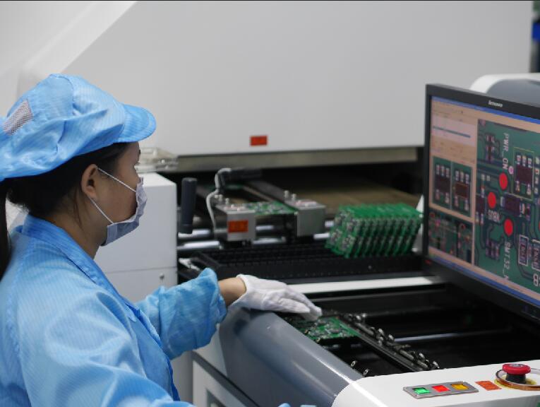
The challenge is to find a way to thoroughly test a fully populated circuit in a timely, cost-effective way, without compromising signal integrity. Depending on the technology, the challenge can be as simple as making minor design changes, which actually can happen at the Gerber level versus requiring a significant revision to the board in question. First let’s conquer the simple. For analog, RF, and lower technology digital boards, the approach is the simplest. Typically, straightforward flying probe test is the answer. The better EMS companies use a dual-sided flying probe tester as shown in Figure 1. For this test approach, the test engineer simply asks that the vias not be covered with soldermask, which can be a simple change handled at the CAM/Gerber level. Because flying probe testers can generally test an via with a 20 mil pad and a 10 mil hole, the holes do not need to be plated shut. Depending on the test coverage, the test department may recommend adding vias, assuming the design can handle it from an electrical perspective.
Many CAD systems can add the via as a test point. One via per net provides 100% access, increasing the odds for very good actual test coverage. If vias are being avoided, as in sensitive analogs or RF technology boards, the tester maybe able to test at the solder joint. The challenge with this approach is many sensitive analogs or an RF design can minimize the size of the pad, increasing the chances of testing at the lead and not the pad. This should be avoided due to the risk of damaging the component. Also the customers need to be open minded about “witness marks” left behind by the tester. Harder solder—for example lead-free—reduces this problem.
Testing this technology typically results in higher test coverage approaching 100%. Higher-technology product can pose a much more significant challenge. The technology in this class includes high-speed digital, via in pad, blind buried vias and high BGA count. The curveball in this case is the number of circuits that actually never see an external via, making it impossible to probe the circuit. The previous advice still applies: Try to have a via exposed for every circuit. This includes making sure they are not covered by a component or soldermask. Test coverage can be enhanced if the engineer allows all exposed vias to be unmasked. This approach will give the test engineer options to test the circuit; solving common problems like testing around tall components. Typically, this result in “okay” test coverage, but no one wants to be just okay!
Superior test coverage on this type of product includes the use of boundary scan (JTAG) technology to significantly increase the test coverage as well as reduce test time. Stating the obvious, this presumes that the components on the board are boundary scan capable. Assuming this is the case, the five signal boundary scan daisy chain circuit needs to be connected. Generally, the electrical engineer connects them, but not for test purposes. Instead it is seen as a method for programming components. It is important to note that the original intent of boundary scan was to test and not program; however, it is used more often for programming. Implementing boundary scan for test can be no different than your current programming routine. Simply connecting the chain opens up the possibility of test, and is a great beginning but only the beginning. It is recommended that a test engineer who specializes in boundary scan test review the schematic before layout begins. Doing so typically will yield a faster, more thorough test. Test throughput also increases by removing all circuits tested at boundary scan from the flying probe test program. This approach has been used on boards with more than 35,000 test points, which resulted in 95% test coverage. So the challenge has been met. It is possible to have a highly tested product built in the United States at an affordable price. Amazingly, what has been outlined here requires less upfront and design work than the traditional bed of nails in-circuit test and can be used in all phases of development, including prototype, pilot and production runs.
The original article comes from PCB007/SMT magazine.March 2016
get more information about Edadoc PCBA/SMT process: http://www.en.edadoc.com/Cases/Show/137


